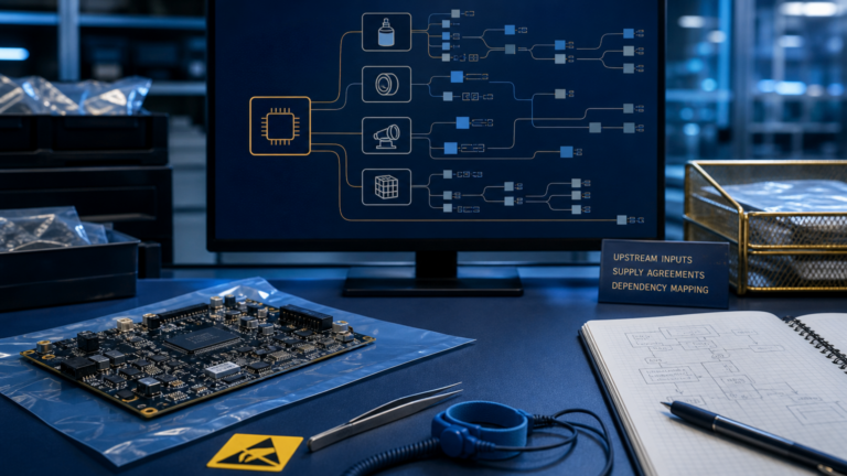
Advancing Cu-Cu Hybrid Bonding
As the world of technology continues to evolve, the demand for more efficient and advanced semiconductor packaging grows. With the advent of 3D Cu-Cu Hybrid Bonding technology, the industry is poised to address the limitations of conventional flip-chip soldering. Advanced semiconductor packaging is intricate and challenging, and transformative solutions are revolutionizing the supply chain industry. As semiconductors become smaller and more powerful, the focus on miniaturization and advanced packaging technologies is growing.
The Challenges of Bump Scaling
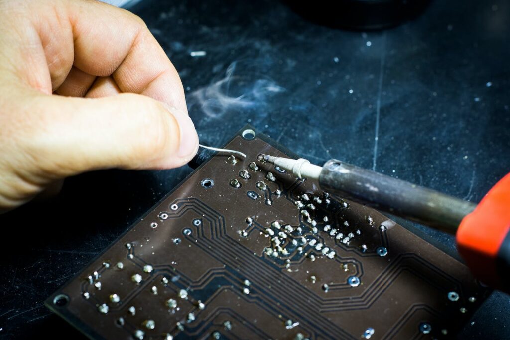
As the industry pushes towards miniaturization, the size of solder bump pitches becomes an increasing concern. Smaller bump pitches bring about several challenges, from establishing reliable electrical connections to avoiding manufacturing errors. Additionally, the industry has to deal with etching difficulties and electrochemical deposition plating complexities.
To overcome these–the industry is transitioning towards Thermocompression Bonding (TCB), a method offering promise for fine-pitch bonding applications. While TCB presents an answer to some challenges, it introduces others. As the contact pitch reduces further, risks associated with solder balls, such as intermetallic compound formation and bridge failures, increase. These challenges become more pronounced in high-performance component packaging scenarios.
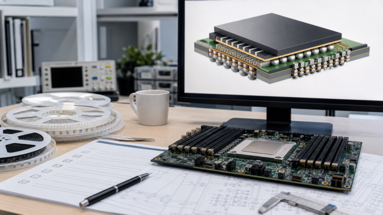
The Emergence of Cu-Cu Hybrid Bonding
Enter Cu-Cu Hybrid Bonding technology–a solution that promises to revolutionize semiconductor packaging. This technology offers several advantages over flip-chip soldering, from enabling ultra-fine pitches and reducing parasitic capacitance to allowing for more compact and efficient semiconductor packages. Despite its promise, Cu-Cu Hybrid Bonding technology has its challenges. The manufacturing process requires precise control and innovative methodologies to ensure a clean dielectric surface and handle thin wafers. Development efforts focus on refining these aspects to pave the way for broader adoption of this technology.
The Future of Cu-Cu Hybrid Bonding

As the industry continues evolving, so will Cu-Cu Hybrid Bonding technology. Efforts are underway to hone the manufacturing process and tackle challenges associated with die singulation, contamination, and thin-wafer handling. Through these advancements, the industry is on track to create smaller, more powerful, and energy-efficient electronic devices.
The world of semiconductor packaging is complex and ever-evolving. Through innovations like Cu-Cu Hybrid Bonding, the industry continually pushes the boundaries of what is possible. For more in-depth analysis and to stay abreast of the latest trends, check out more from the PCX blog. It offers comprehensive insights into the past, present, and future of advanced semiconductor supply chain, packaging, and industry news. At Pacific Component Xchange, we provide readers with the knowledge they need to navigate this rapidly changing landscape.