Tata-ASML Dholera Partnership Gives Buyers a Ramp-Execution Signal
Tata Electronics and ASML have added a concrete lithography-support signal to India’s Dholera fab story. For component buyers, the useful takeaway is not that near-term supply has changed. It is that the ramp path for a future regional foundry source now has another named equipment and process-support partner behind it.
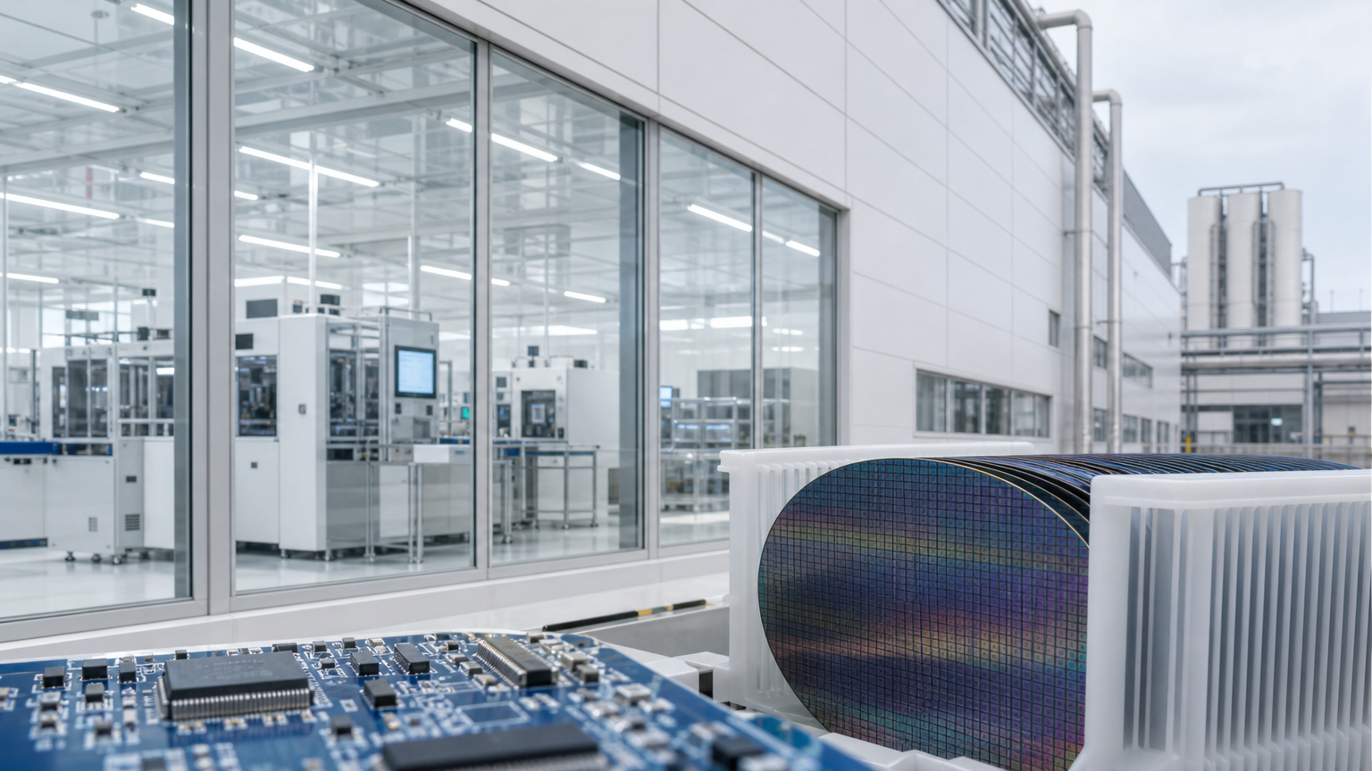
Evertiq reported on May 18 that Tata Electronics and ASML signed a memorandum of understanding tied to Tata’s upcoming 300 mm semiconductor fab in Dholera, Gujarat. The original Tata Electronics release says ASML will support establishment and ramp-up of the fab with lithography tools and solutions, local talent development, supply-chain resilience initiatives, and R&D infrastructure.
The practical signal for buyers is specific: this is a ramp-execution and ecosystem-development milestone. It should be tracked by teams with long-life integrated circuits, power management ICs, memory, analog, logic, microcontrollers, connectors, passive components, and discrete semiconductors on future demand plans. It should not be converted into an assumption that current open orders, spot availability, lead times, or approved-source lists have changed.
What the Tata-ASML announcement says
The announcement centers on Tata Electronics’ planned commercial 300 mm fab in Dholera and ASML’s lithography role in that project. Evertiq summarized the collaboration as a plan to deploy ASML’s suite of advanced lithography tools and solutions for the Dholera facility. Tata’s own release adds that the two companies will cooperate on domestic talent, supply-chain, and research initiatives that support the long-term success of the fab.
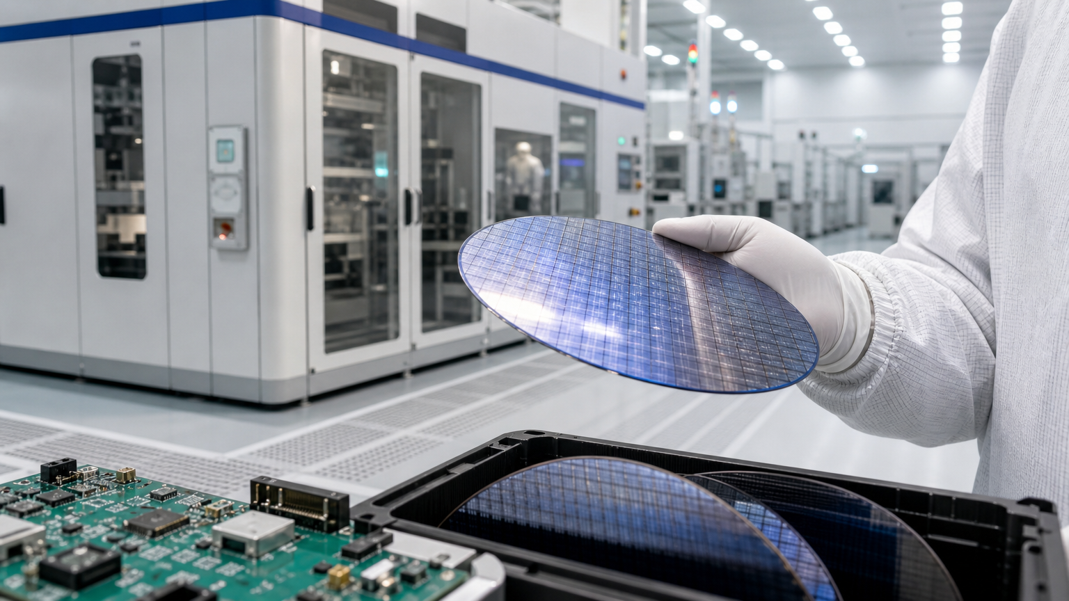
That distinction matters. Lithography capability is one of the core manufacturing requirements in a semiconductor fab, and equipment-support partnerships can reduce uncertainty around ramp execution. But the release language is about establishment, ramp-up, training, R&D infrastructure, and ecosystem development. It does not say that qualified devices are already moving into commercial distribution, that any board-level part has a new source of supply, or that lead times have improved for buyers today.
What this means for PCX buyers
For PCX buyers, the announcement belongs in the planning file, not the emergency-buy file. Procurement teams should treat it as one more signal that India’s semiconductor manufacturing ecosystem is becoming more structured. That may matter over time for approved-vendor strategy, regional resilience, and future sourcing optionality.
The near-term sourcing work remains part-specific. Buyers still need to review the exact MPNs on the BOM, the node and package used by those devices, qualification requirements, approved alternates, lifecycle status, and the customer’s tolerance for changes. A fab partnership may eventually support more regional manufacturing options, but it does not automatically qualify a replacement IC, MCU, MOSFET, diode, memory device, sensor, or power-management component for an existing design.
Why lithography support matters to a fab ramp
Tata’s release frames ASML’s role around lithography tools and solutions, training, supply-chain resilience, and R&D infrastructure. Those are not cosmetic details. A fab ramp depends on equipment installation, process stability, yield learning, skilled operators, local engineering depth, and a surrounding supplier ecosystem. A named lithography partner can therefore make the project more credible as a long-term manufacturing signal.
For sourcing teams, however, credibility is not the same as availability. The steps between a fab partnership and purchasable components include process qualification, customer design wins, device-level production, packaging and test capacity, reliability validation, commercial channel decisions, and customer approvals. Each step can affect timing. Each step is also different by component family: an automotive analog IC, an industrial MCU, a power device, and a consumer-market logic device do not create the same buyer risk.
What not to assume yet
The safest reading is deliberately narrow. Do not assume this partnership changes current lead times for integrated circuits, memory, power management ICs, discretes, connectors, relays, switches, passives, or electromechanical parts. Do not assume it reduces pricing pressure in any present component family. Do not assume it creates a second source for a specific BOM line unless the manufacturer, distributor, qualification file, and customer documentation support that conclusion.
The Tata release does include useful project context. It says the Dholera fab is planned as India’s first 300 mm commercial fab, names a planned total investment, describes target application areas including automotive, mobile devices, AI, and other segments, and refers to access to process nodes through a PSMC partnership. Those are useful for understanding strategic direction. For a public sourcing article, they should remain context rather than a basis for unsupported near-term market claims.
Which current BOMs may still need attention
The best buyer response is a focused BOM review. Start with long-life programs that may still be in production when new regional capacity becomes relevant. Then separate parts by risk category: sole-source ICs, aging analog and power-management devices, constrained memory or logic lines, alternates that require firmware or board changes, and components with documentation or traceability requirements.
Buyers should also ask whether the project’s likely future output overlaps their actual component exposure. A regional fab signal may be strategically important without touching the exact device family on today’s BOM. If the current risk is a discontinued controller, an allocation-sensitive MOSFET, a hard-to-find connector, a legacy memory device, or a passive component with a specific package and tolerance, the right action is still part-level sourcing work, not a broad conclusion about fab news.
| Buyer question | Why it matters |
|---|---|
| Which exact MPNs are exposed? | Fab announcements do not map cleanly to existing BOM lines without device-level evidence. |
| Are alternates already approved? | Future capacity helps only if qualification and documentation paths are ready. |
| Which parts are long-life or lifecycle-sensitive? | Programs with long support windows may benefit most from tracking regional capacity milestones. |
| Is urgency raising quality risk? | Any open-market sourcing response still needs inspection, traceability, and documentation discipline. |
Buyer takeaway
The Tata-ASML partnership is a meaningful semiconductor ecosystem signal. It points to maturing lithography support around the Dholera fab and gives buyers another milestone to monitor in India’s regional manufacturing build-out. The sourcing conclusion should stay measured: track the ramp, but do not rewrite current availability assumptions until there is part-level evidence.
If a capacity headline raises questions about current exposure, PCX can help buyers review the exact MPNs, alternates, lifecycle constraints, and documentation requirements before acting. For active sourcing pressure, send PCX the parts list for BOM review and sourcing support so the discussion starts with the actual BOM rather than a broad market headline.