
Roadmap progress is real. It is just not the same thing as near-term board-level relief.
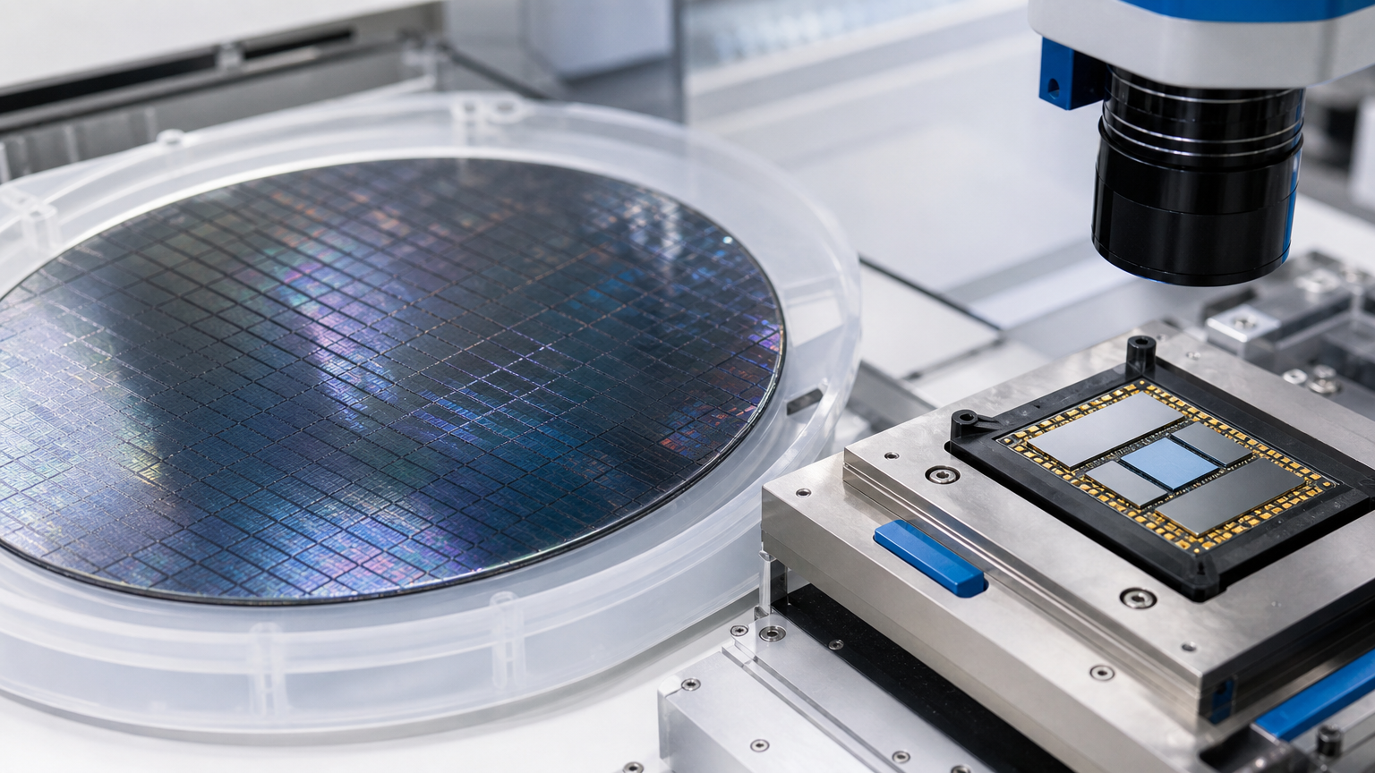
Advanced-node news is easy to overread. TSMC has extended its roadmap through the end of the decade, Intel has put 18A into shipped client silicon, and Samsung says its 2nm program remains on track for second-half 2026 mass production. Those are meaningful milestones. They show where engineering effort, capital spending, and customer demand are concentrating.
But a procurement team still has to ask a narrower question: does this change what we can actually buy, qualify, and build around now? In many cases, the answer is no, or at least not yet. The gap between a process-node milestone and a board-ready supply outcome can still be defined by packaging, equipment lead times, substrate availability, outsourced assembly-and-test capacity, or the simple fact that an existing BOM does not live on that node in the first place.
What the latest announcements actually say
The current signal set is stronger than the seeded demo copy this plan started from. Tom’s Hardware reported from TSMC’s 2026 North America Technology Symposium that the foundry is now discussing A14 for 2028, A13 and A12 for 2029, and an N2U extension of the 2nm family. Intel said at CES 2026 that Core Ultra Series 3 is the first compute platform built on Intel 18A and that the platform is already powering more than 200 PC designs, including edge and industrial use cases. TrendForce, citing Samsung’s fourth-quarter 2025 discussion, reported that Samsung still targets second-half 2026 mass production for 2nm and 2029 for 1.4nm.
Those are not fake milestones or marketing fluff. They matter because they show which foundries are converting roadmap language into actual production steps. They also help buyers see that advanced-node progress is happening on different clocks. Intel has a shipping product. Samsung still frames 2nm as an upcoming ramp. TSMC is already extending the discussion past N2 into later generations.
| Signal | What it supports | Why it is not immediate BOM relief |
|---|---|---|
| TSMC roadmap through A12/A13/A14 | Long-range node planning and customer alignment | Most milestones are still tied to 2027-2029 production windows |
| Intel 18A client launch | A concrete example of advanced-node silicon reaching products | A shipped client platform does not remove unrelated packaging or mature-node constraints elsewhere |
| Samsung 2nm mass-production target | Foundry readiness moving toward the next ramp | Yield, customer programs, and downstream product timing still matter after the headline |
What it may change later
These milestones do matter for medium-term planning. If your team builds around high-end compute, data-center infrastructure, optical interconnect, or next-generation accelerator programs, the roadmap tells you where ecosystem pressure is going next. IEEE Spectrum’s March 2026 coverage of DWDM light engines for AI infrastructure is a good example. The technology is moving closer to co-packaged optics and scale-up networking, which means future system designs will depend on more than a smaller transistor geometry alone.
That matters for supplier strategy. Over the next several planning cycles, advanced-node progress can reshape package choices, memory attachment strategies, power density assumptions, thermal design, and test flows. It can also change where buyers should expect the next concentration of demand, especially when AI and hyperscale programs are absorbing a disproportionate share of advanced manufacturing attention.
In other words, roadmap news belongs in the long-horizon planning file. It can influence which programs deserve earlier supplier conversations, where engineering should expect qualification work, and which categories may become strategically important even before they become broadly available.
What it probably does not change now
The near-term constraint story is still more complicated than wafer-node progress. EE Times reported in April that TSMC expects to spend nearly $56 billion in 2026 and still may not fully catch demand by 2027, while CEO C.C. Wei emphasized that fabs take years to build and additional time to ramp. Electronics Weekly, citing TrendForce, said bottlenecks in 3nm-2nm wafers and 2.5D/3D advanced packaging still persist, with CoWoS remaining tight and only expected to ease somewhat by 2027.
That is the key filter for buyers. A process roadmap can improve, and even a production ramp can begin, while real product availability remains constrained by packaging throughput, substrates, equipment, memory, or outsourced assembly capacity. EE Times also reported that ASE expects advanced-packaging sales to double in 2026 as TSMC shifts more work toward OSAT partners, with some meaningful outsourcing gains only stepping up in the second half of 2026 and into 2027.
If you are buying outside the small set of programs that actually consume these leading-edge nodes, the headline may have even less immediate effect. Existing industrial, communications, and embedded builds may still be driven by mature-node logic, power-management devices, memory choices, connectors, or qualification rules that do not improve simply because a frontier node advanced.
Which current BOMs may still need attention
This is where a practical filter helps. First, identify whether the exposed line items on your BOM are actually tied to advanced-node roadmaps or whether they sit in adjacent categories such as memory, power management, interface ICs, or legacy logic. Second, check whether the risk is front-end wafer availability or a back-end issue such as packaging, substrate, or test capacity. Third, separate design optimism from approved-vendor reality: a future package or node is only useful once your engineering, quality, and customer requirements can accept it.
For teams reviewing semiconductor exposure, PCX’s integrated circuits category page is a practical starting point for mapping which device families are actually involved in the conversation. The goal is not to react to every roadmap slide. The goal is to build an exact MPN list, note which parts are currently quoted or constrained, and decide whether the next action is monitor, quote, qualify an alternate, or buy early.
- Review exact MPN exposure before treating roadmap news as supply relief.
- Ask suppliers whether the limiting step is wafer, package, substrate, memory, or test.
- Flag programs with long qualification cycles, because those rarely benefit from headline timing alone.
- Document a revisit date tied to actual production windows rather than broad media excitement.
Buyer takeaway
The right conclusion is not that advanced-node news is meaningless. It is that buyers need to classify it correctly. TSMC, Intel, Samsung, packaging houses, and photonics suppliers are all giving the market useful signals. Those signals help procurement teams understand where capital is going and where future competition for capacity may build. They do not automatically tell you that this quarter’s availability assumptions are safer.
For PCX customers, the disciplined move is to translate roadmap headlines into a BOM review. If a current build depends on exact component availability, alternate approval, lifecycle timing, or a constrained supplier base, use the roadmap as one input, not the answer. When that review needs a sourcing cross-check, send PCX the exact MPNs for a BOM review and sourcing support discussion.