10M02SCE144C8G
$7.81
FPGA – Field Programmable Gate Array non-volatile FPGA, 101 I/O, 144EQFP
10M02SCE144C8G – 2K LE Non-Volatile MAX® 10 FPGA – Altera
This Altera MAX® 10 FPGA delivers flexible, instant-on processing in a compact 144-pin package. Engineered for embedded systems requiring reliable reprogrammable logic, it features non-volatile configuration, 101 I/O pins, and low-power operation. PCX ensures genuine Altera components with same-day shipping and technical support.
Key Features
- 2000 Logic Elements for complex digital designs
- Non-Volatile Configuration – No external boot memory required
- 101 I/O Pins – Flexible interface options
- 110Kb Embedded Memory – On-chip data storage
- 2.85V–3.465V Operating Voltage – Power-efficient performance
- 0°C to 85°C Industrial Temp Range – Robust operation
Technical Specifications
This surface-mount FPGA integrates 125 LABs/CLBs in a 144-EQFP package (20x20mm). It features 110,592 RAM bits for on-chip data buffering and operates at industrial temperature grades (TJ). The device supports instant-on functionality and in-system programmability via its 101 I/Os. Download full datasheet for design implementation details.
Typical Applications
- Industrial control systems and motor drives
- Communications infrastructure interfaces
- Medical monitoring devices
- Automotive sensor processing modules
- IoT edge computing gateways
About Altera
Altera (now part of Intel) pioneered programmable logic solutions with over 35 years of innovation. Their FPGAs set industry benchmarks for reliability, power efficiency, and design flexibility across aerospace, telecommunications, and industrial automation sectors.
MAX® 10 FPGAs represent Altera’s commitment to cost-optimized, non-volatile solutions. With built-in flash memory and analog integration, these devices simplify system architecture while maintaining full FPGA reprogrammability for future-proof designs.
About FPGAs
Field Programmable Gate Arrays provide hardware-customizable digital circuits that outperform fixed-function processors in parallel processing tasks. Unlike ASICs, FPGAs can be reconfigured post-deployment, enabling rapid prototyping and field updates without hardware changes.
These devices are essential for applications requiring real-time signal processing, protocol bridging, or algorithm acceleration. Their parallel architecture handles multiple operations simultaneously, making them ideal for vision systems, encryption, and high-speed data acquisition where deterministic latency is critical.
Packaging
Available in protective trays for automated assembly. Contact PCX for reel packaging options and MOQ details.
FAQs
Q: Does this FPGA require external configuration memory?
A: No – its non-volatile architecture stores configuration in on-chip flash.
Q: What development tools support the MAX® 10 series?
A: Altera Quartus Prime software (free web edition available) with MAX 10 device support.
Q: Can I reprogram this in-circuit?
A: Yes – supports full in-system programmability via JTAG or active serial interfaces.
Q: What’s the difference between LE and logic gates?
A: One LE ≈ 15-20 ASIC gates – this 2000 LE device handles ~30k gate equivalents.
Q: Is the 110Kb memory user-accessible?
A: Yes – configurable as RAM, ROM, or FIFO buffers.
Q: Does PCX provide lifecycle status updates?
A: Yes – we actively monitor Altera’s product lifecycle and notify customers of changes.
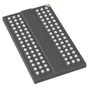
⚠️ Note: Product image is representational – verify markings upon receipt.
Ready to Integrate? Order Today for Fast Delivery!
Get genuine Altera 10M02SCE144C8G FPGAs shipped same-day from PCX’s verified stock. Our specialists ensure component authenticity and provide technical documentation support. Contact us now to secure your units!
Additional Information
| Category | Integrated Circuits (ICs)EmbeddedFPGAs (Field Programmable Gate Array) |
|---|---|
| Brand | Altera |
| Mfr | Altera |
| Series | MAX® 10 |
| Packaging | Tray |
| Part Status | Active |
| DigiKey Programmable | Not Verified |
| Number of LABs/CLBs | 125 |
| Number of Logic Elements/Cells | 2000 |
| Total RAM Bits | 110592 |
| Number of I/O | 101 |
| Voltage - Supply | 2.85V ~ 3.465V |
| Mounting Type | Surface Mount |
| Operating Temperature | 0°C ~ 85°C (TJ) |
| Package / Case | 144-LQFP Exposed Pad |
| Supplier Device Package | 144-EQFP (20×20) |
| Full Description | 10M02SCE144C8G |