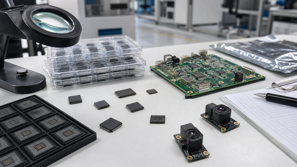
Paras Semiconductors’ planned OSAT facility in Madhya Pradesh belongs in a narrower sourcing file: sensor, optical, and optronic packages that may depend on specialized assembly and test routes. The inspected public record points to a memorandum of understanding, a proposed investment, and a strategic direction around advanced semiconductor packaging. It does not say that a specific integrated circuit, sensor device, memory part, connector, passive component, or board-level assembly is easier to buy today.
That narrower lens matters. Packaging and test capacity can become a real constraint for sensor-heavy and optical designs, but the buyer decision is still made at the level of exact MPNs, package requirements, qualification status, documentation, and delivery timing. For PCX buyers, the practical value of the Paras signal is to identify exposed lines early and keep alternate-source and verification work ahead of urgency.
What changed
Evertiq reported that Paras Semiconductors, a subsidiary of Paras Defence and Space Technologies, signed an MoU with the Madhya Pradesh government’s science and technology department to jointly set up an OSAT facility in the Indore-Ujjain region. Evertiq also reported that the company said the investment would be ₹62 billion, or about $643.8 million, and that the proposed facility would focus on advanced semiconductor packaging and testing.
ETGovernment also reported the buyer-relevant details in more precise terms. It says Paras Semiconductors signed an MoU with the Government of Madhya Pradesh on July 22, 2026, to establish an advanced semiconductor packaging OSAT facility. It also says the state allotted fifty acres on the Ujjain-Indore Corridor and describes a proposed ₹6,200 crore investment.
What this means for PCX buyers
For buyers, the signal is less about one future site and more about where packaging, test, and qualification capacity may become part of the sourcing conversation. The filing says Paras Semiconductors is focused on advanced semiconductor capabilities for strategic and high-performance sensor applications, including sensor technologies, optical and optronic systems, and other strategic applications in the near term. It also says the facility could support future expansion into AI chips and other advanced semiconductor technologies as market opportunities evolve.
That is a useful prompt for a targeted BOM review. Procurement teams supporting aerospace, defence-adjacent, industrial sensing, optical modules, embedded control, or high-reliability assemblies should identify which line items depend on specialized packages, test flows, or supplier qualification paths. A packaging headline may not change today’s RFQ result, but it can change the questions buyers ask about second sources, lifecycle exposure, and how much schedule risk sits outside wafer fabrication.
Why OSAT signals matter before parts appear on a buy list
Outsourced semiconductor assembly and test capacity sits between wafer output and usable components. A design may have wafer capacity available, but buyers still need qualified package formats, test capacity, documentation, traceability, and a supplier route that matches the end application. That is especially relevant for integrated circuits used in sensor, optical, optronic, RF, power-management, and board-level control designs where package, thermal, and test requirements are part of the real sourcing risk.
The BSE filing frames the Paras project as part of a broader semiconductor ecosystem that includes manufacturing, advanced packaging, design, testing, research, electronics manufacturing services, talent development, and trusted supply chains. PCX should not turn that ecosystem language into an availability promise. It is better read as a planning signal: buyers can map which assemblies are exposed to advanced-package and test dependencies before a shortage, redesign, or last-time-buy event forces a rushed decision.
How to file the signal without over-reading it
The safest sourcing-file interpretation is disciplined and narrow. The Paras announcement supports a conclusion that India is continuing to build domestic semiconductor packaging ambition and that Paras wants to place sensor and strategic-application packaging into that roadmap. It does not support a conclusion that current prices, lead times, allocation status, utilization, or named component availability have changed.
Sourcing teams can still act on the signal without overstating it. Start by tagging affected BOM lines: sensors, optical and optronic devices, specialized integrated circuits, power-management ICs around the subsystem, connectors used in the module, and passive components tied to the board design. Then ask whether any of those items have single-source package dependencies, documentation gaps, end-market qualification requirements, or approved-vendor-list constraints that would make a future packaging or test bottleneck harder to absorb.
What PCX would check next
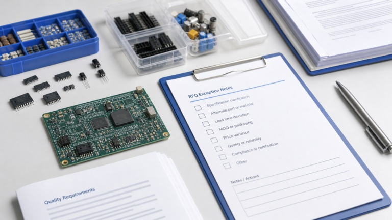
PCX would treat this as a watchlist update, not a buying trigger by itself. The next useful steps are part-level: confirm exact MPNs, package codes, manufacturer lifecycle status, approved alternates, traceability requirements, and whether the program has enough demand visibility for the risk level. Where a customer has urgent need, PCX can help source responsibly through supplier checks, documentation review, and counterfeit-risk controls rather than relying on a broad capacity headline.
This also differentiates the signal from broader advanced packaging roadmap context: the useful question here is not AI infrastructure capacity in general, but whether sensor, optical, and optronic assemblies have package or test dependencies that deserve earlier sourcing review.
The same discipline applies to future updates. If later public sources show equipment delivery, customer qualification, production start, or a component-family impact, the buyer question may change. Until then, the practical takeaway is to keep OSAT, packaging, and test dependencies visible in the sourcing file for strategic sensor and optical BOMs.
Sources and further reading
- Evertiq: Paras to set up $644 million chip packaging facility in India
- ETGovernment: MP govt, Paras Semiconductors sign MoU for ₹6,200 crore OSAT facility
If you are reviewing sensor, optical, optronic, or advanced-package IC exposure on a current build, review PCX integrated circuit sourcing support or send PCX an RFQ with the exact MPN, target date, and documentation requirements.